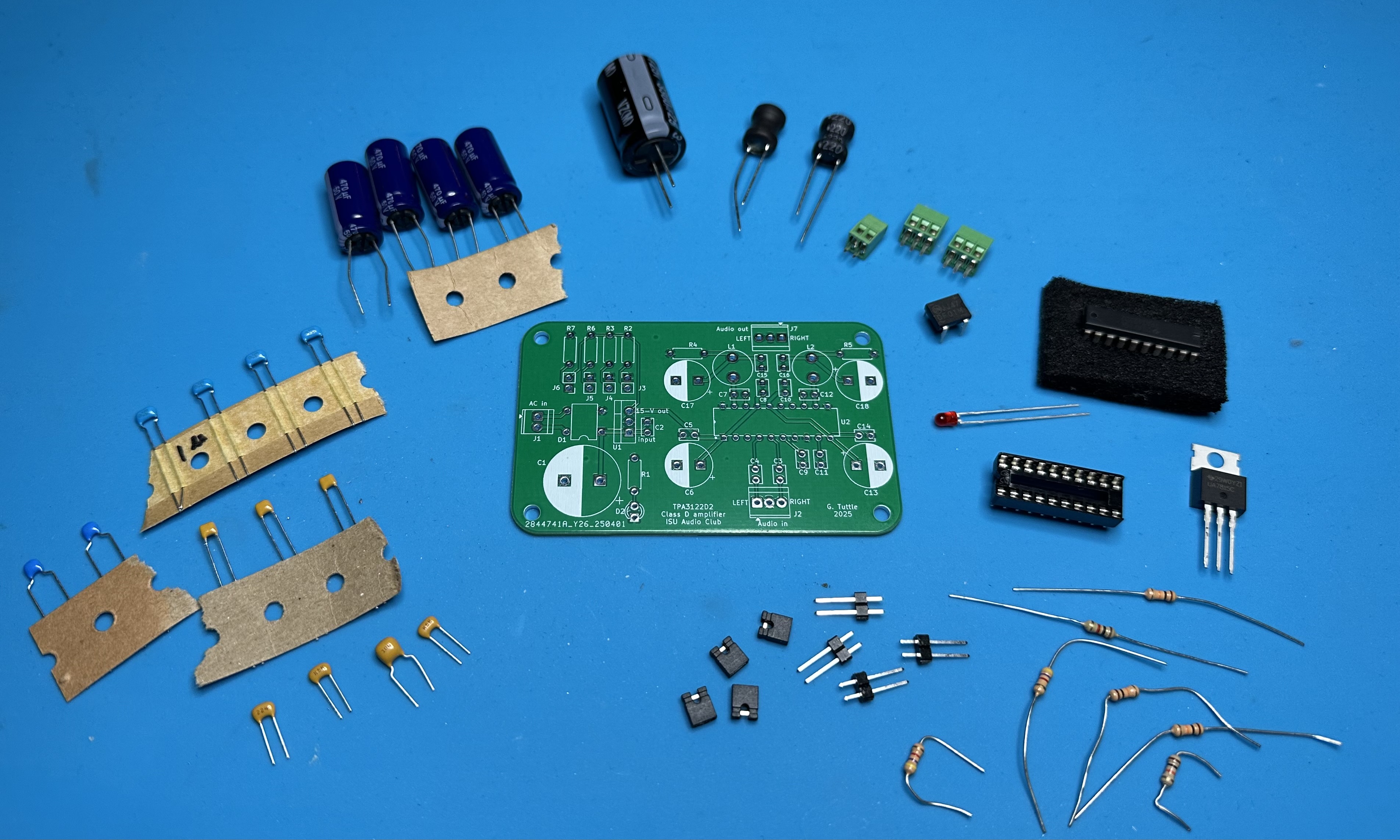
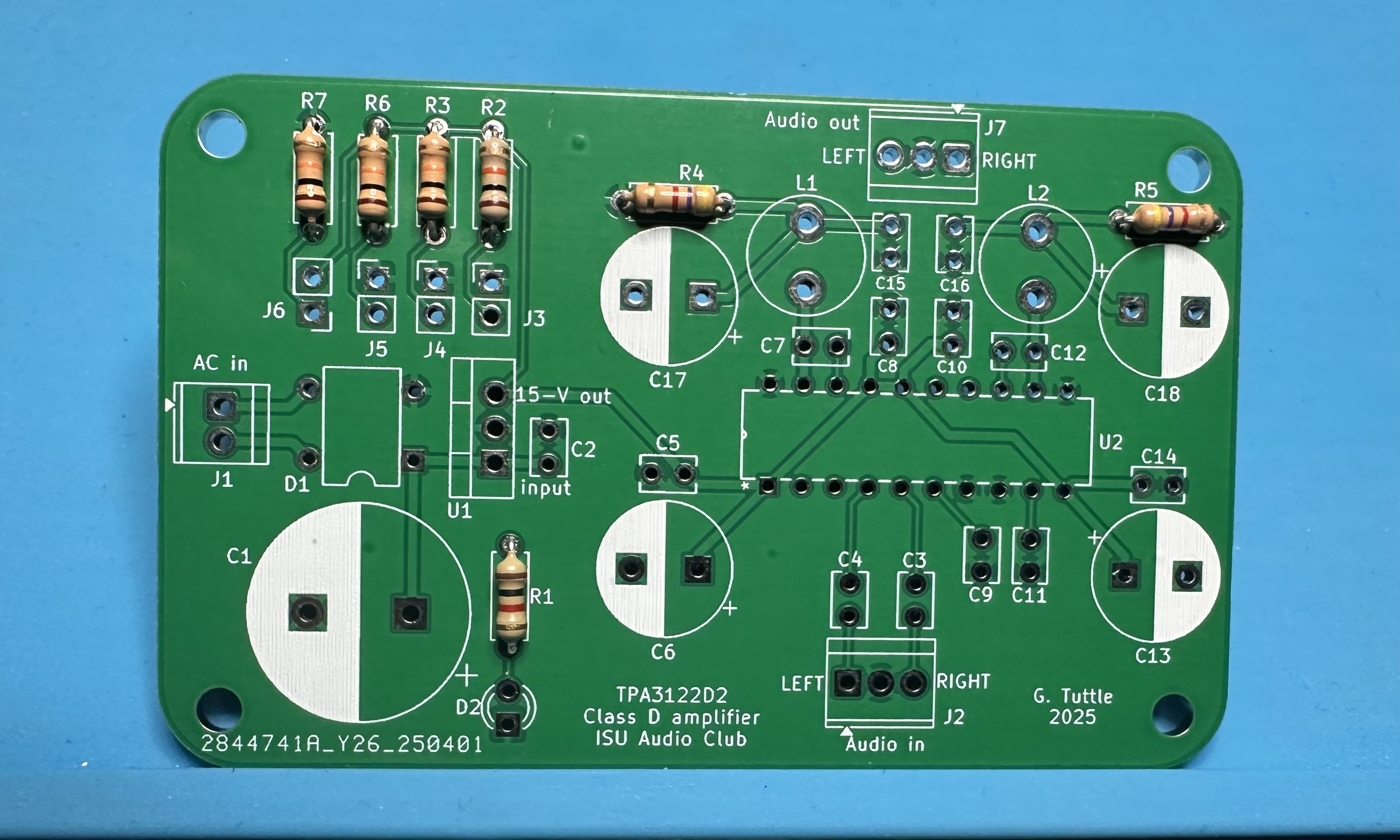
Below are steps for building the class-D amp using the TPA3122 chip from Texas Instruments.
The soldering is straight forward, but this project has a few more parts than some of our earlier projects. In particular, there are lots of capacitors. Make sure that you identify each of the small ones so that you put them into the correct locations. If needed, use the magnifying lamp at the end bench to get a better view of the tiny labels. Or measure the measure the values with the digital multimeter.
All footprints for small capacitors assume a 0.1-inch lead spacing. However, some of capacitors may have 02-inch spacing. In that case, you may need to bend the leads with a pair of pliers so that they will fit.
Note that some parts in the photos below may look slightly different than the ones in your kit. The parts in the photos came from my collection of random stuff, and the parts in your kits came directly from DigiKey.
To get a better view of any photo, open the image in a new window or tab to get a full-sized version.
The usual tools are required: solder and soldering iron, needle-nosed pliers for manipulating parts and pulling leads, and wire cutters for trimming leads after soldering.
- Assemble the parts. (See the BoM for the complete list.)
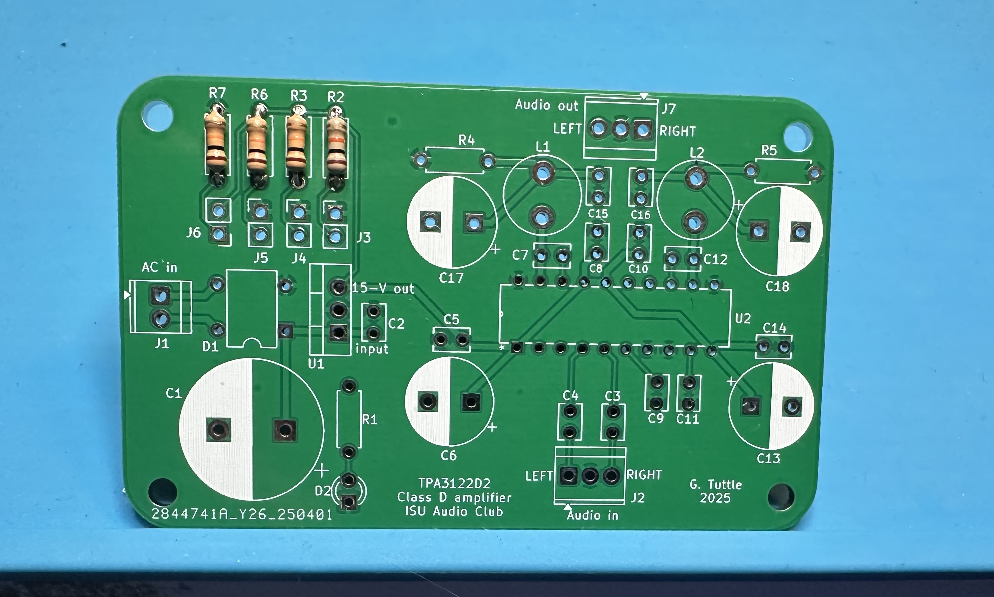
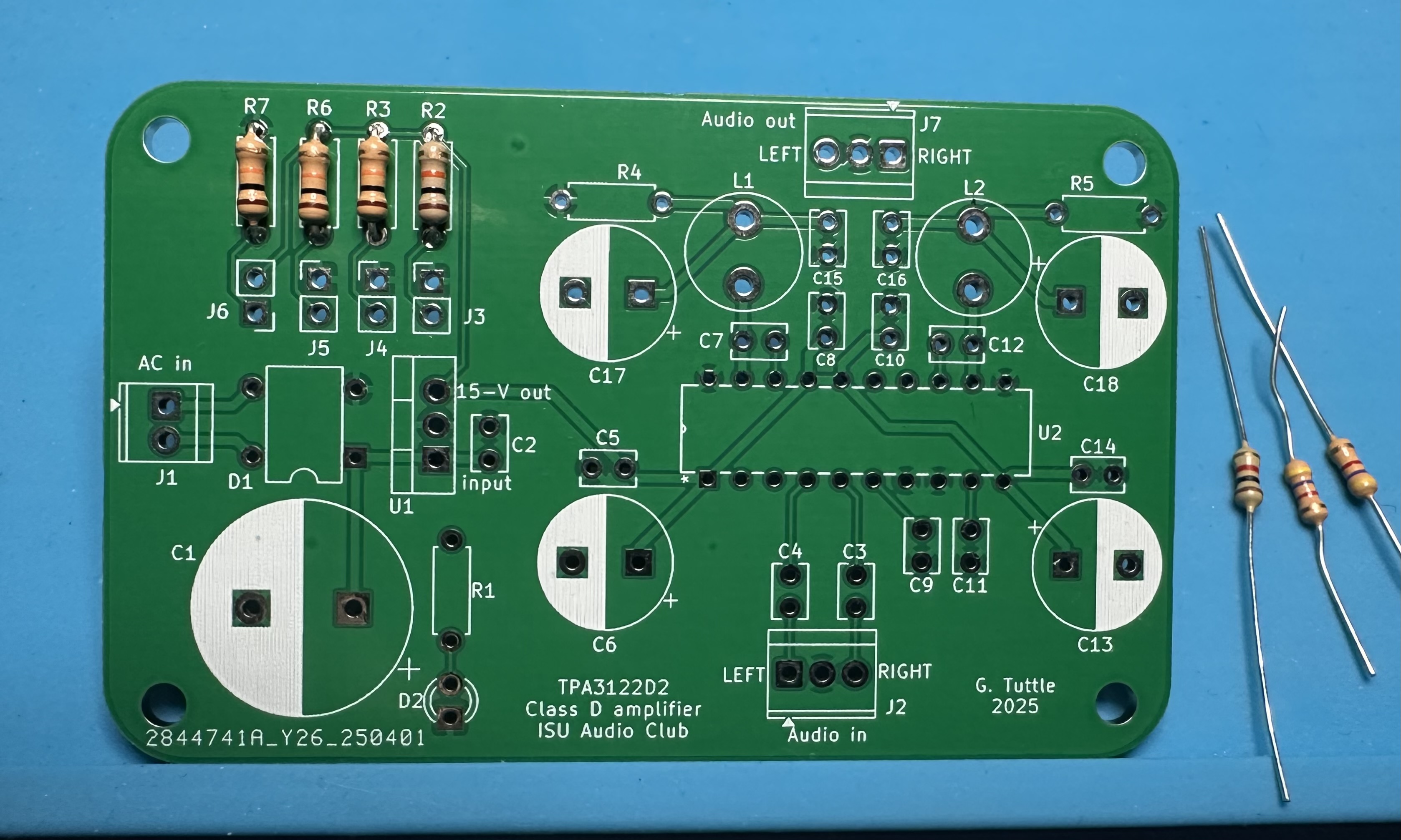
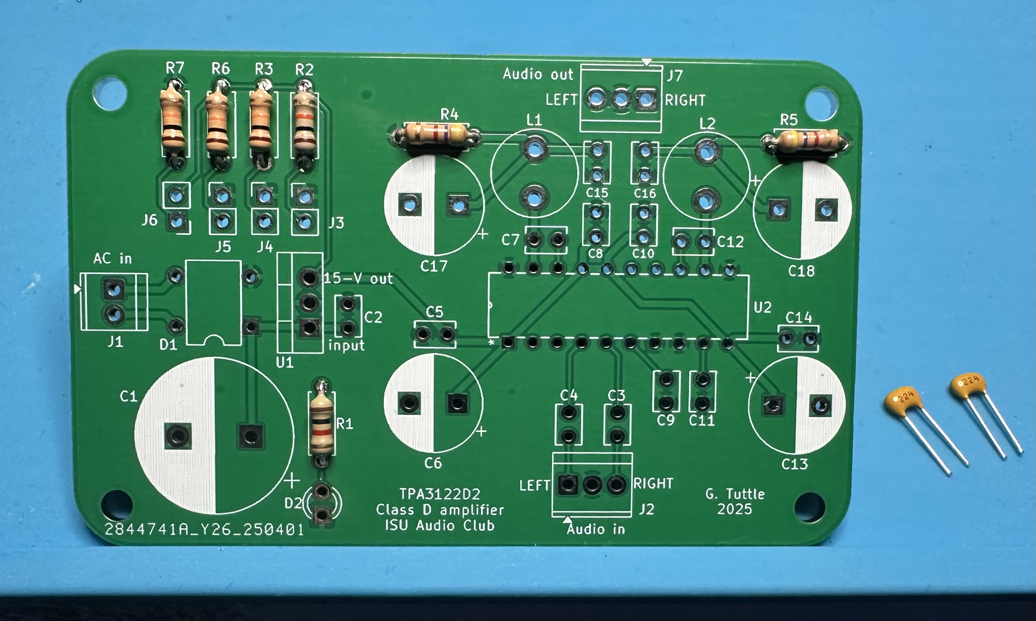
- As usual, we start with the small components and work towards the bigger parts. Solder in the four 10-kΩ resistors, labeled R2, R3, R6, and R7. These are the pull-up resistors used in selecting the gain and activating the mute and shutdown functions of the chip.
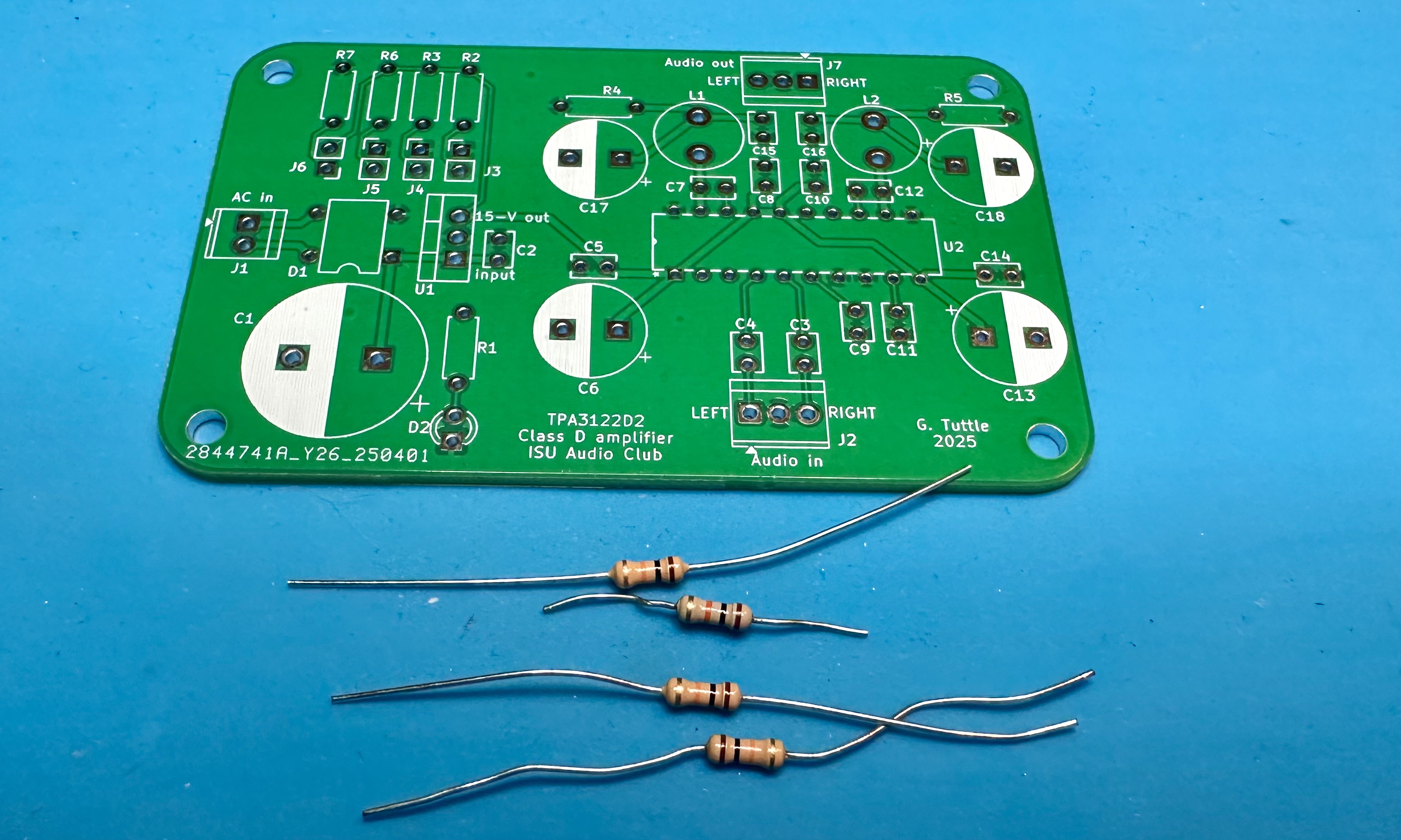
- Now the remaining three resistors: a 1-kΩ resistor for limiting LED current (R1) and two 4.7-kΩ resistors that are in parallel with the output filter capacitor (R4 and R5). (If you choose not to have an LED power indicator, the 1-kΩ resistor can be omitted. Honestly, the 4.7-kΩ resistors could probably be omitted, too.)
- On to the capacitors. Start with the two 0.22-μF (224) capacitors that serve to "boot strap" the MOSFET switches. These are labeled C7 and C12. These are not polarized — they can go in either way.
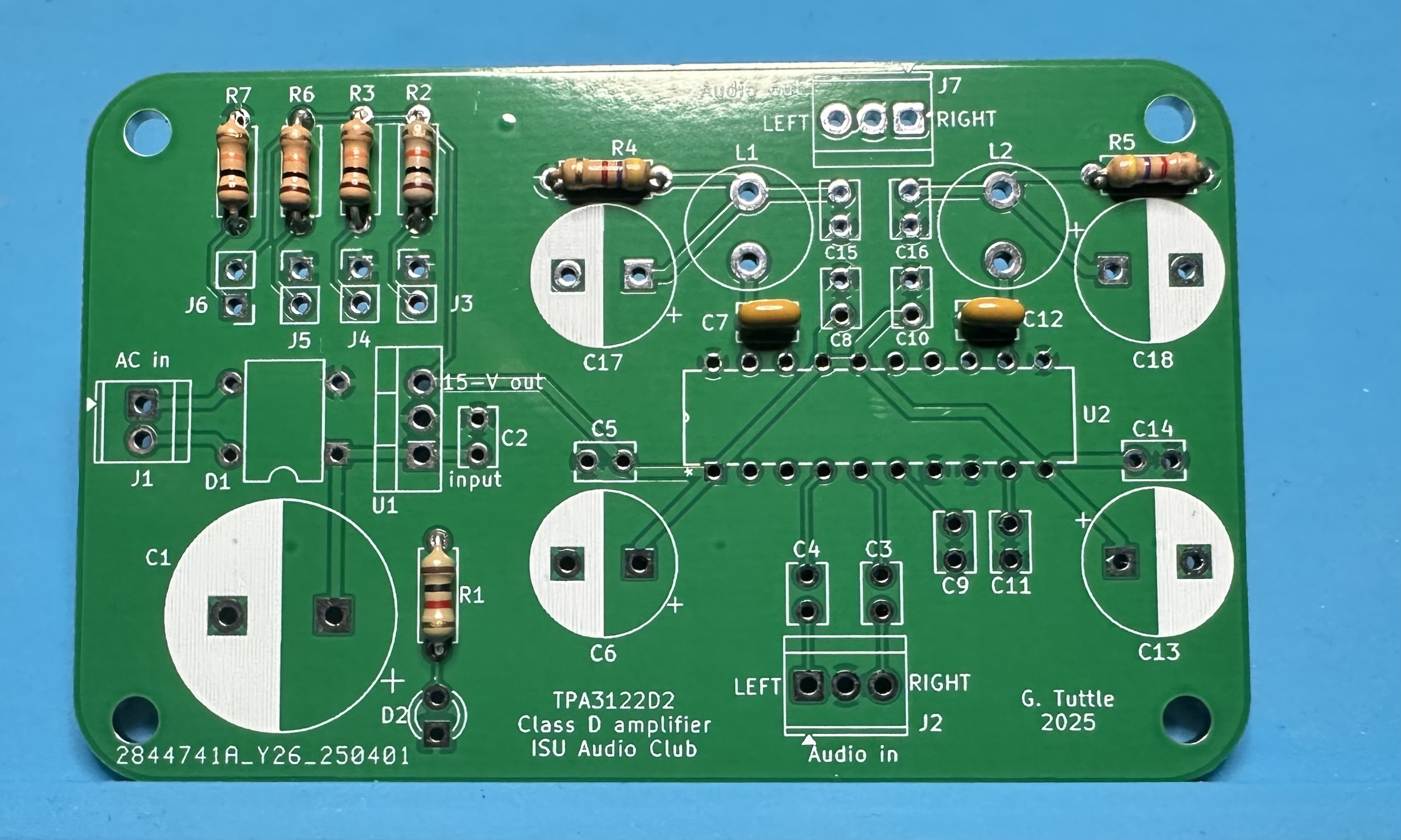
- Now some by-pass capacitors to help smooth out any power supply variations. There is one 10-μF (106) cap that will be located in postion C10 and three 0.1-μF (104) caps for C5, C8, and C14. Note that the 10-μF used here had wider leads (0.2-in separation), and so it was necessary to bend them a bit to fit into the small (0.1-in separation) footprint.
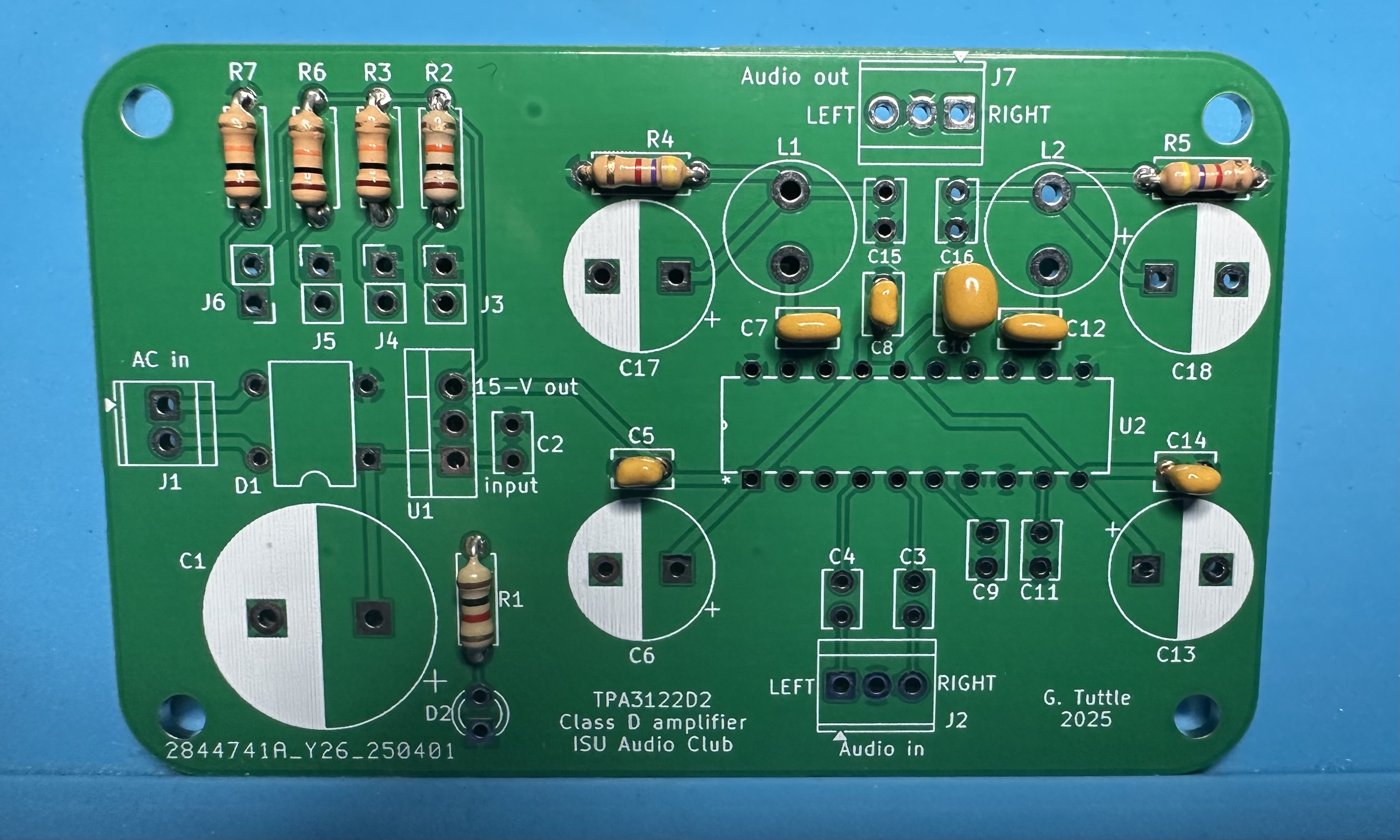
- Next up are the all-important output filter capacitors. These each have a value of 0.68-μF (684) and are labeled C15 and C16 on the board. Note that these also required a bit of "lead re-jiggering".
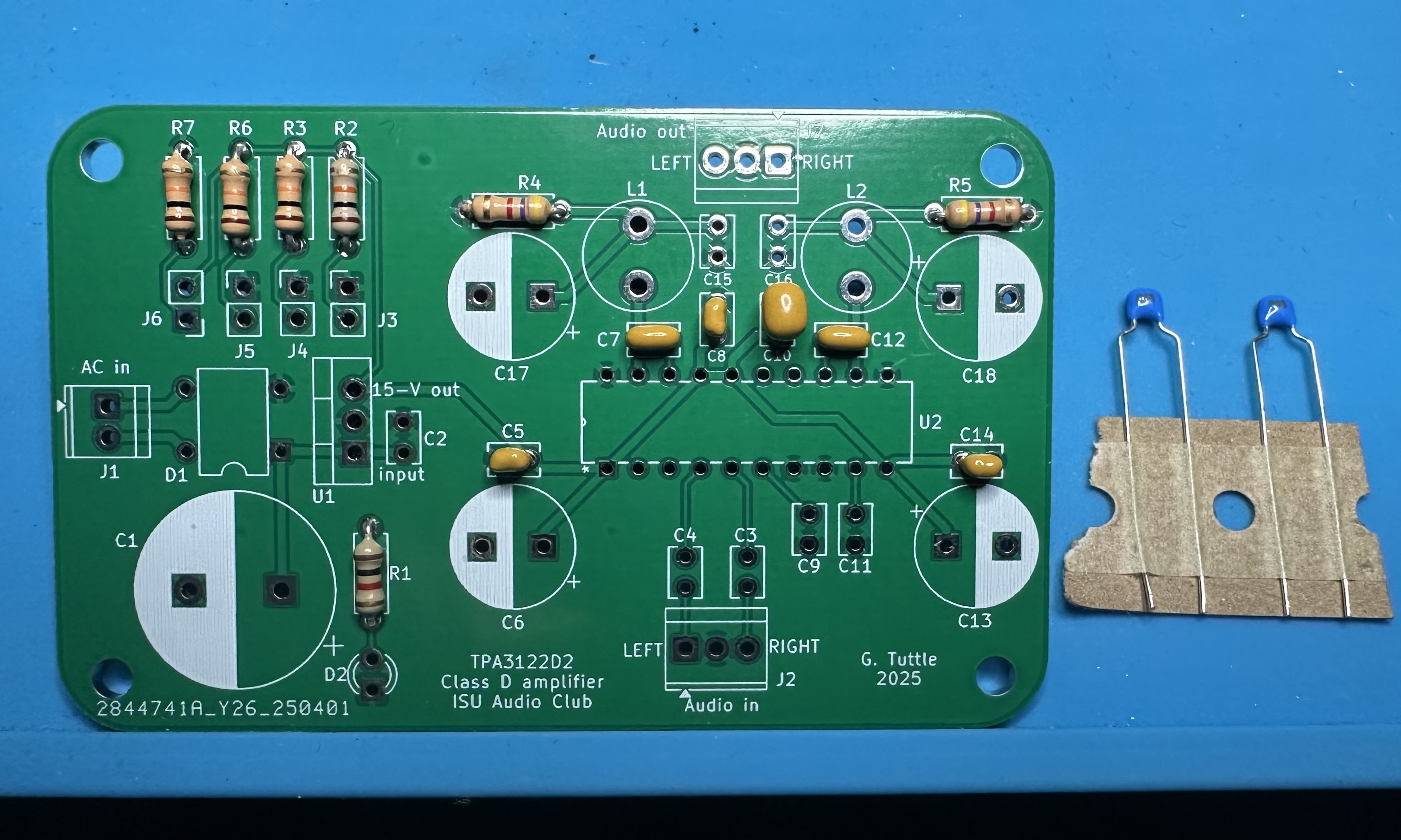
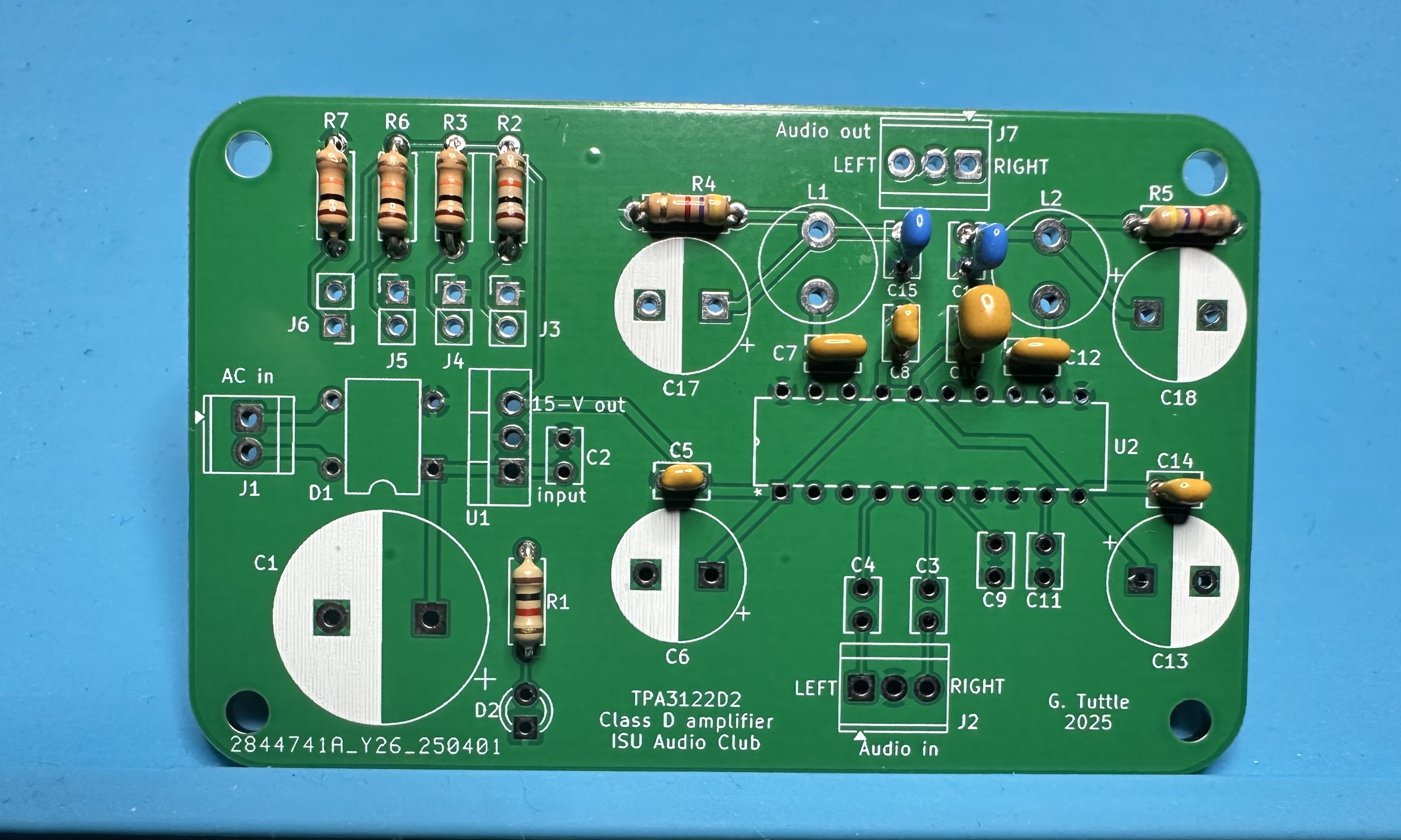
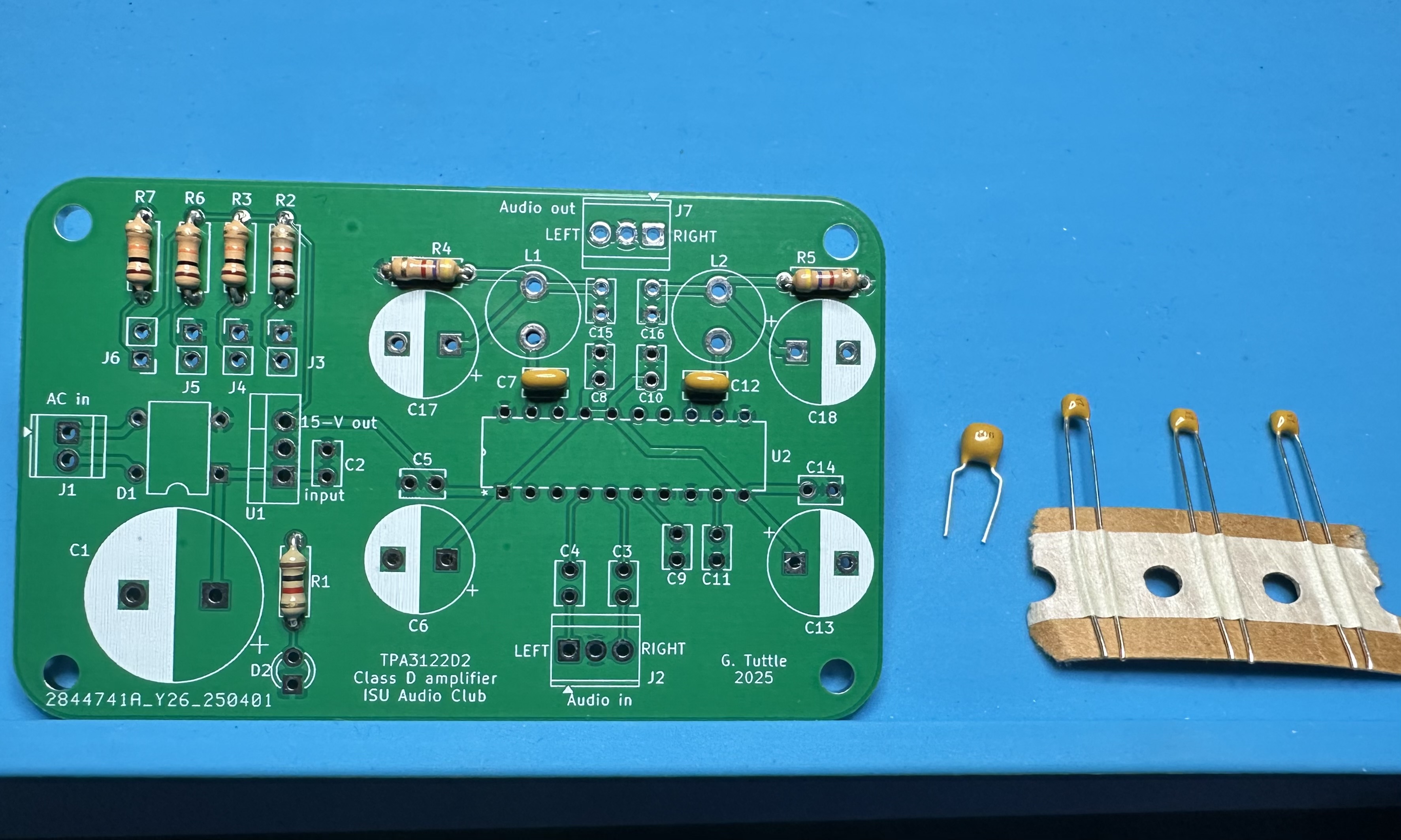
- We can add the four 1-μF (105) capacitors. Two of these, C3 and C4, couple the input signal to the chip. The other two connect to the "VCLAMP" and "BYPASS" pins and are needed for some of the internal operation of the chip.
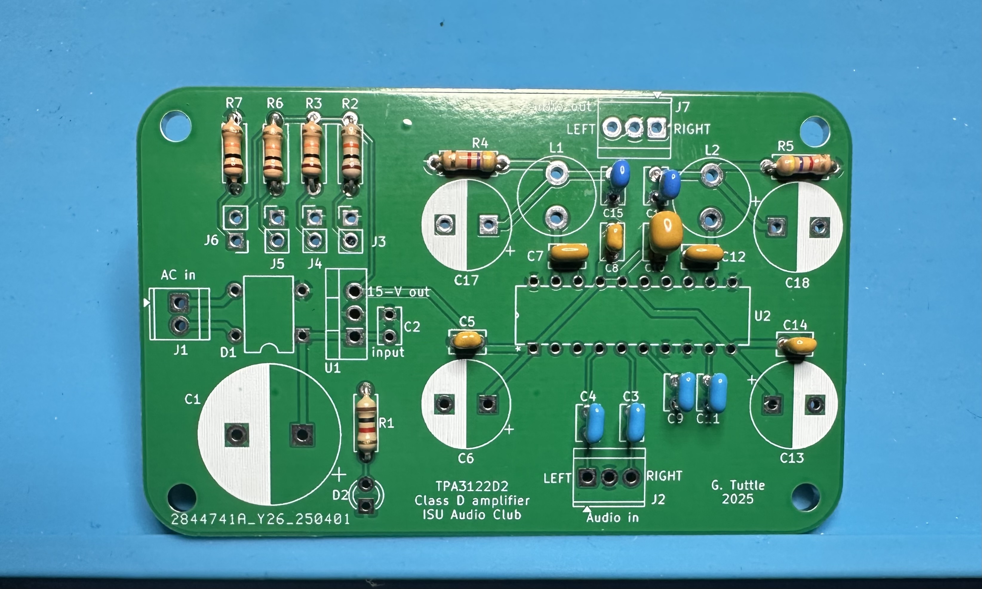
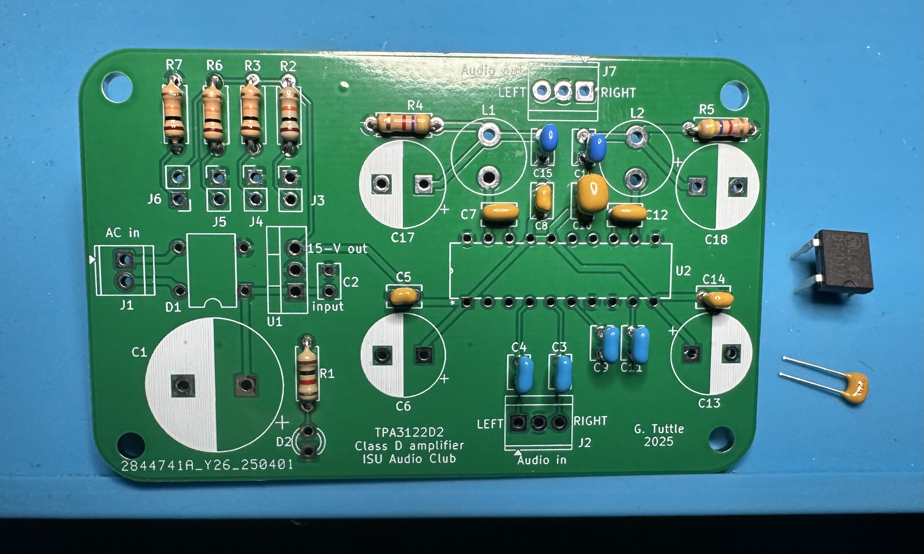
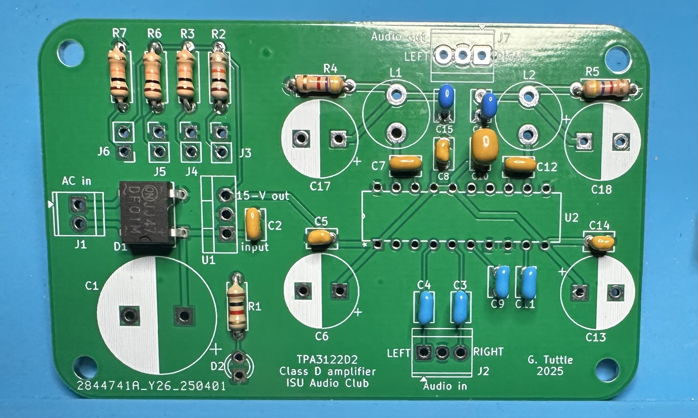
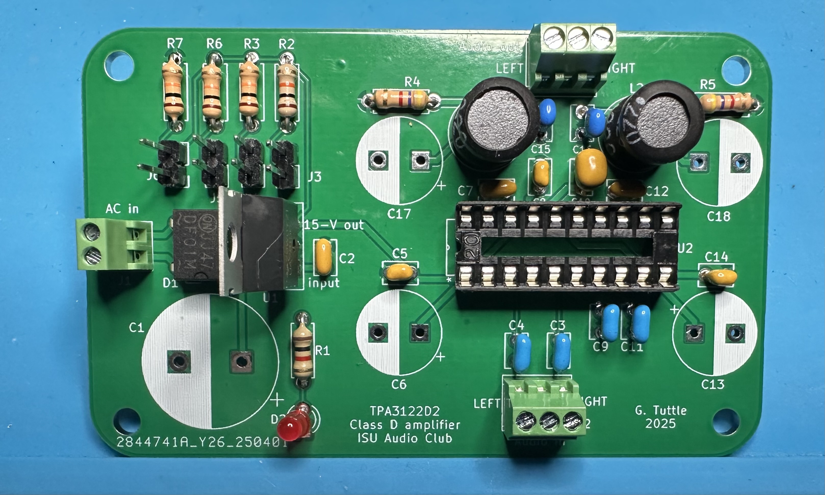
- Now we'll do the last small capacitor and the bridge rectifier needed for the power section. The capacitor has a value of 0.22 μF (224) and is labeled C2 on the board. It's function is to help stabilize the voltage regulator. The bridge rectifier is labeled D1. The cut-out on the footprint outline shows the proper orientation. (Alternatively, the little sine-waves go towards the AC input connector and the +/– go towards the DC voltage regulator.)
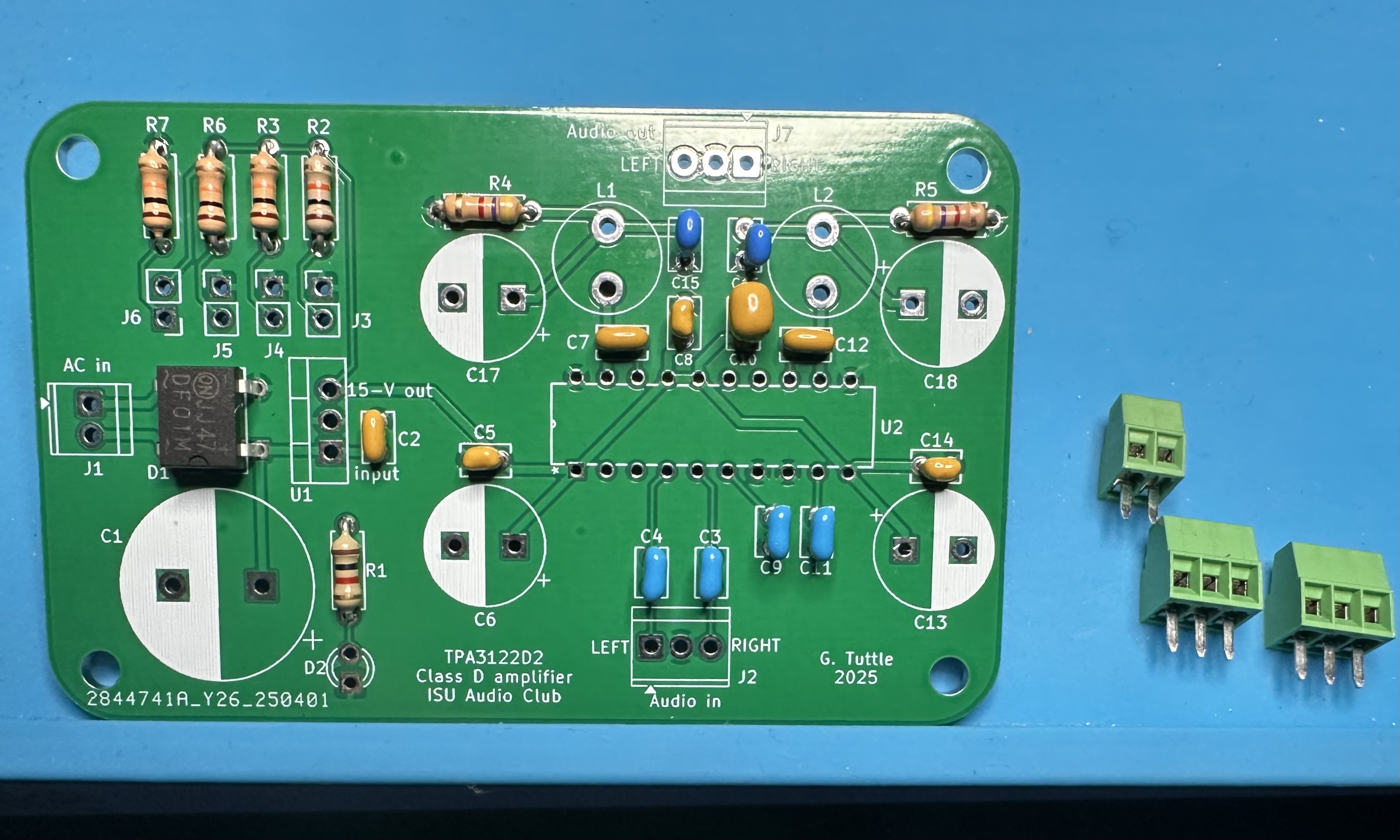
- The three connectors — for power in, audio in and audio out — are up next. Make sure that the openings are to the outside of the board.
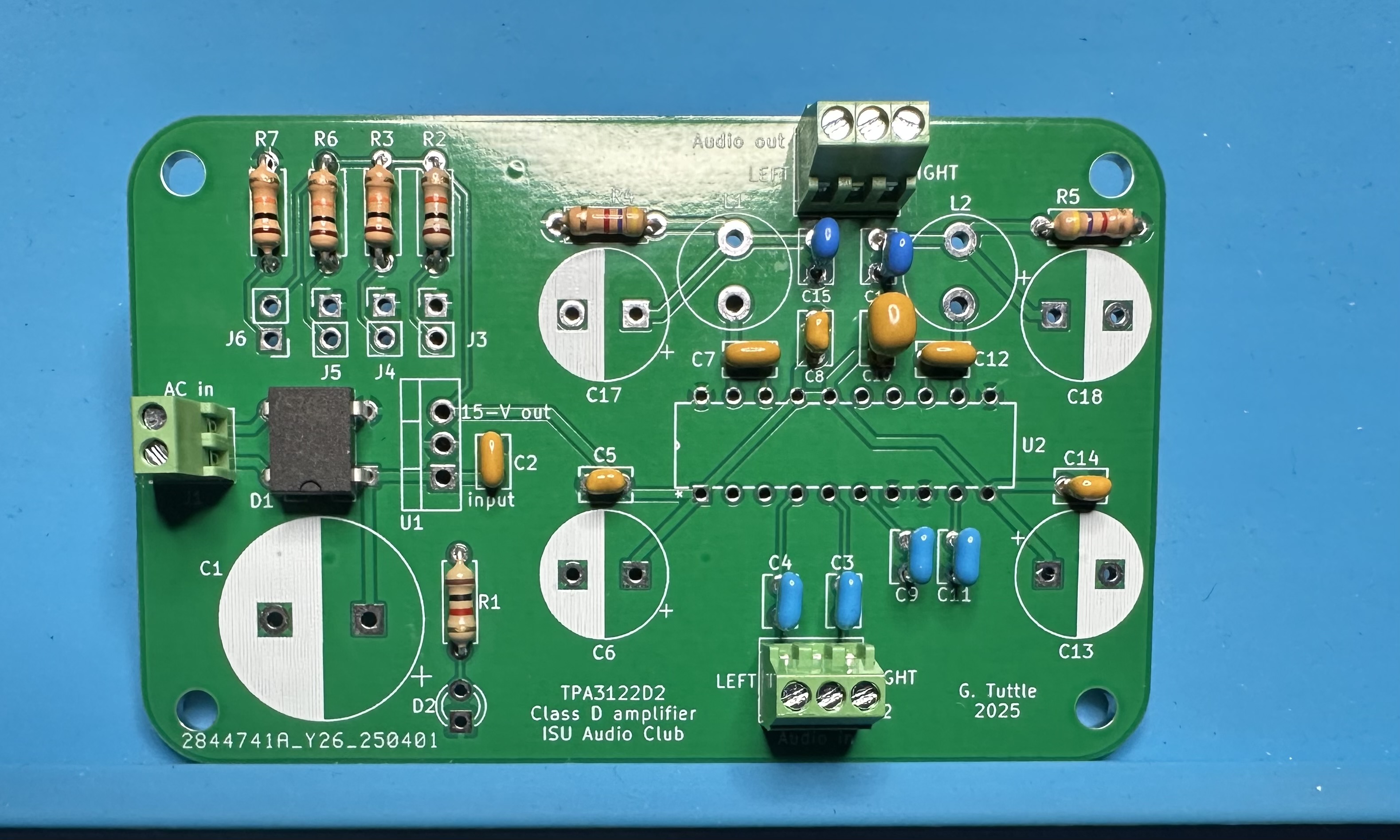
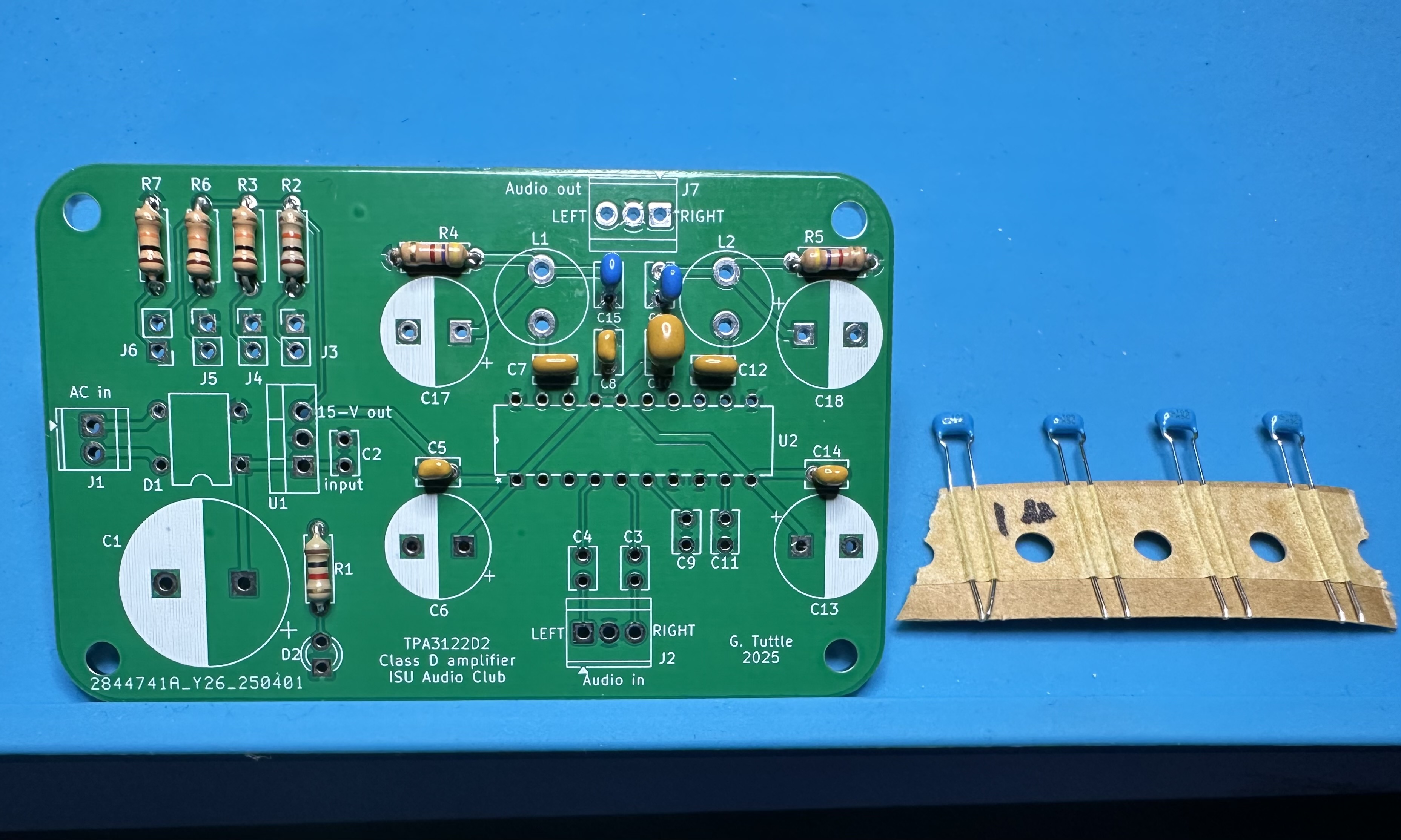
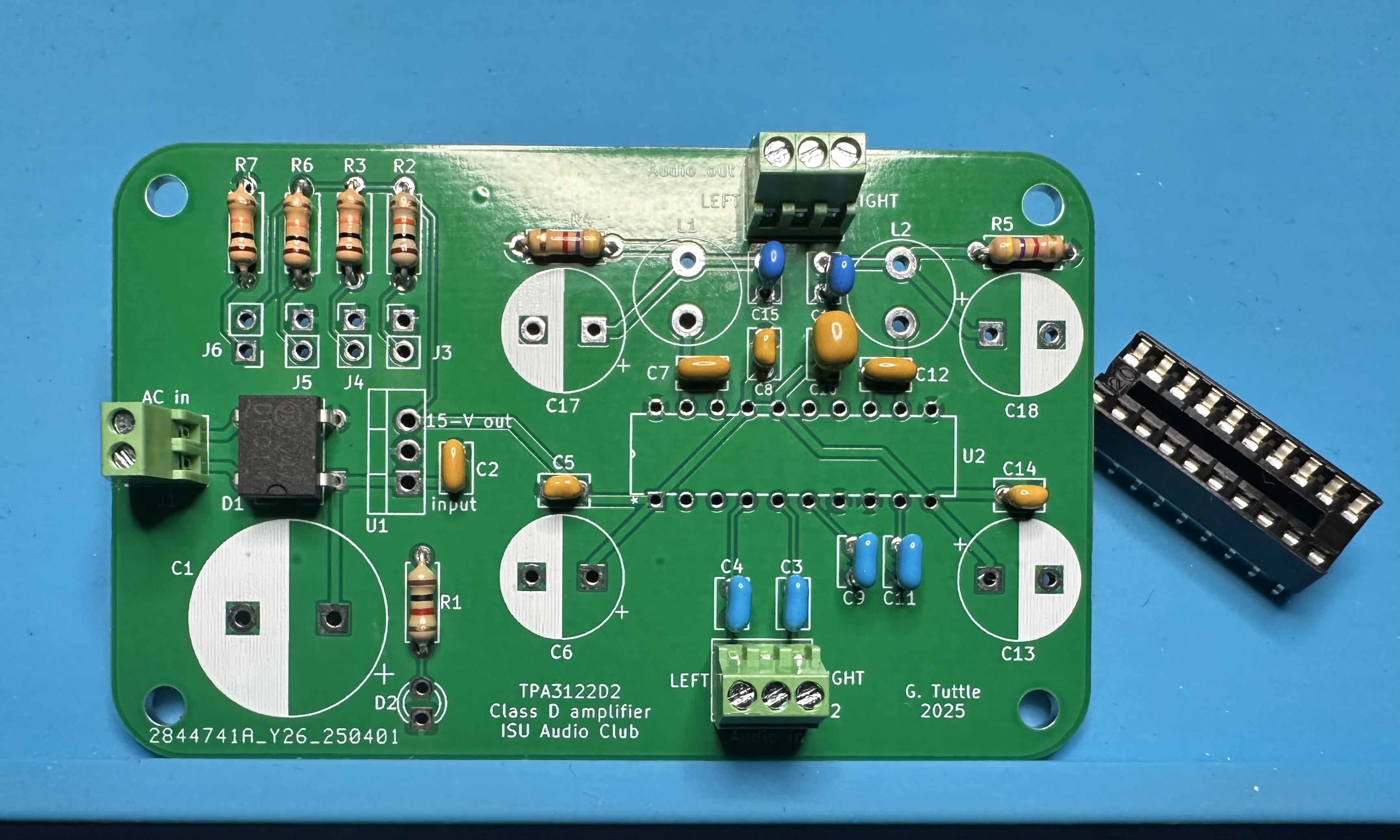
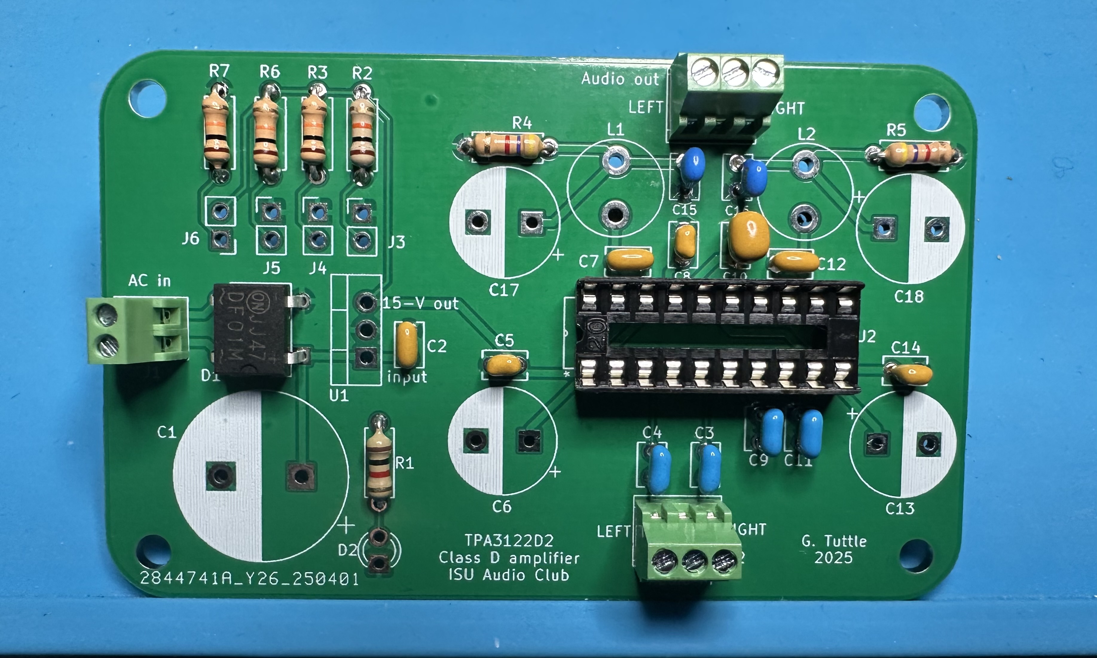
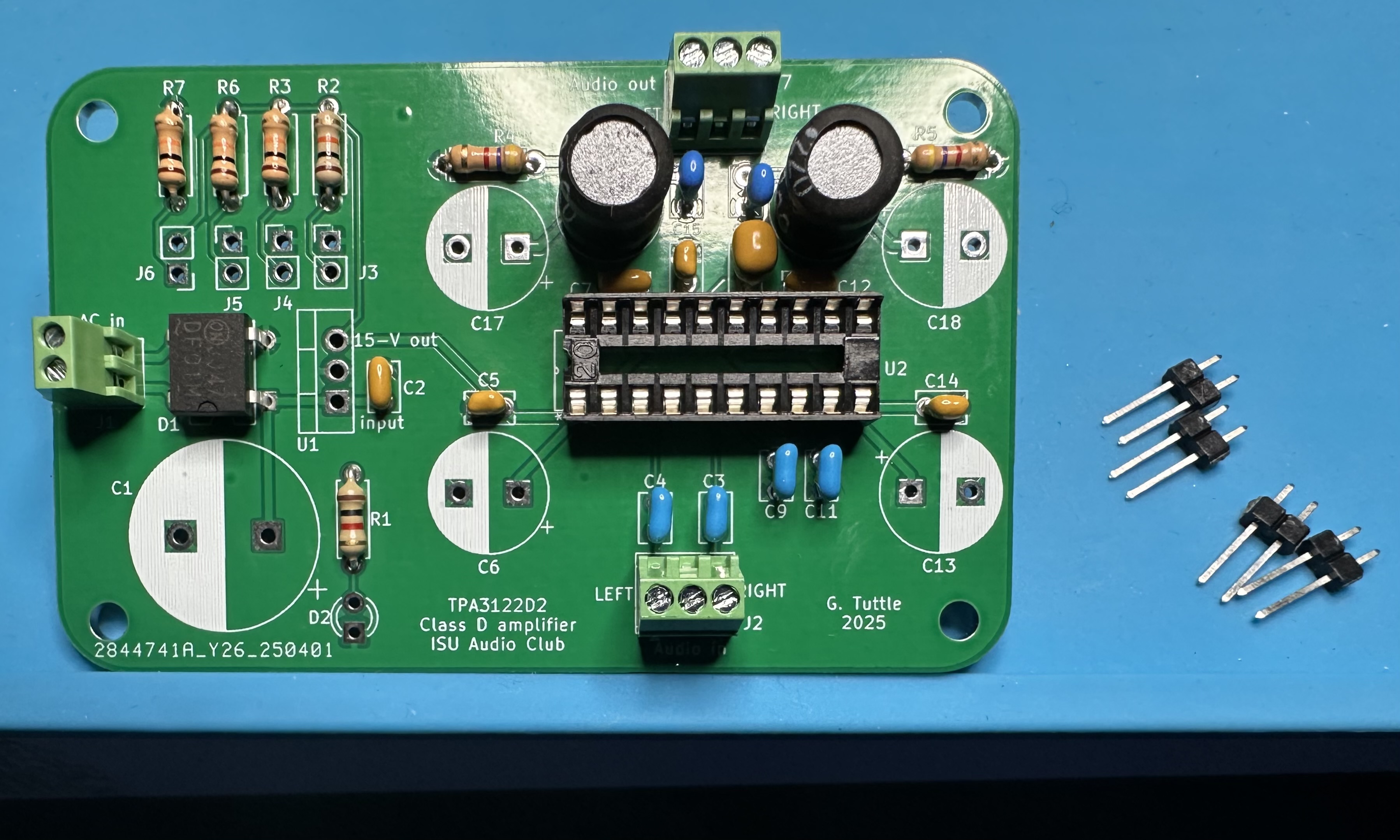
- Solder in the 20-pin socket for the 3122 chip. If are willing to live a bit dangerously, you could skip the socket and solder the chip directly to the board. However, if going that route, it would be best to leave the chip until the end.
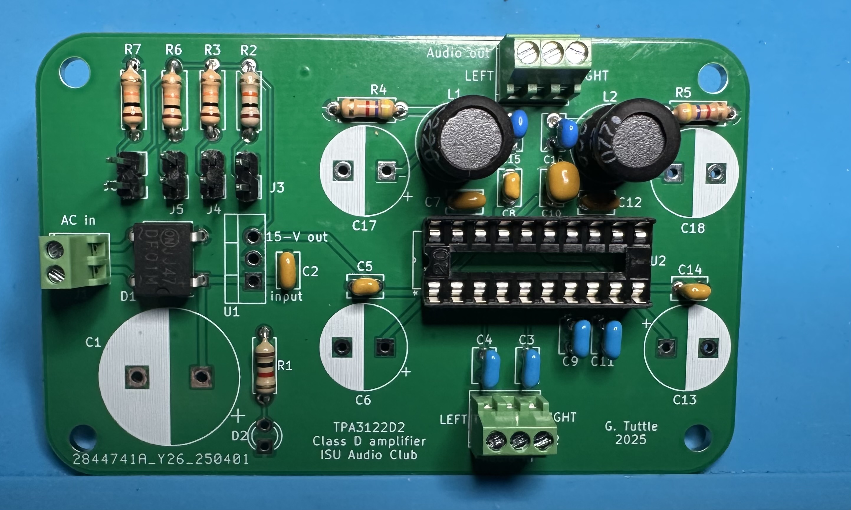
- The parts are getting bigger. Next we can do the two inductors for the output filter. These are labeled L1 and L2.
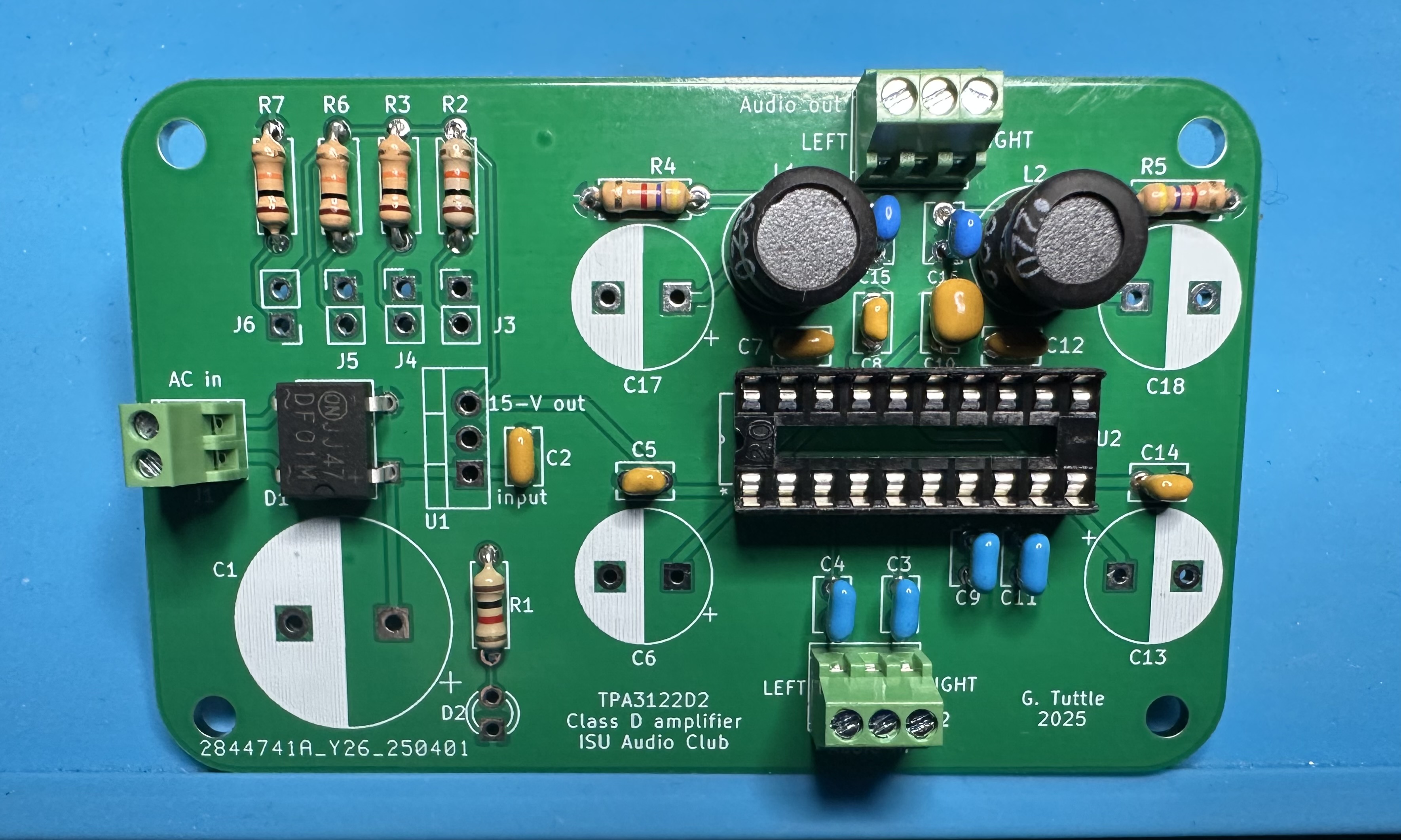
- Let's put in the four pairs of header pins, labeled J3 thru J6. Together with the jumpers to be added later, these serve as selectors to set the gain, and activate the mute and shutdown functions. These can be slightly tricky to solder. It is best to solder one pin initially. Then check the alignment. If it needs to be adjusted, remelt the solder on the pin and fix the alignment. When it looks good, solder the other pin.
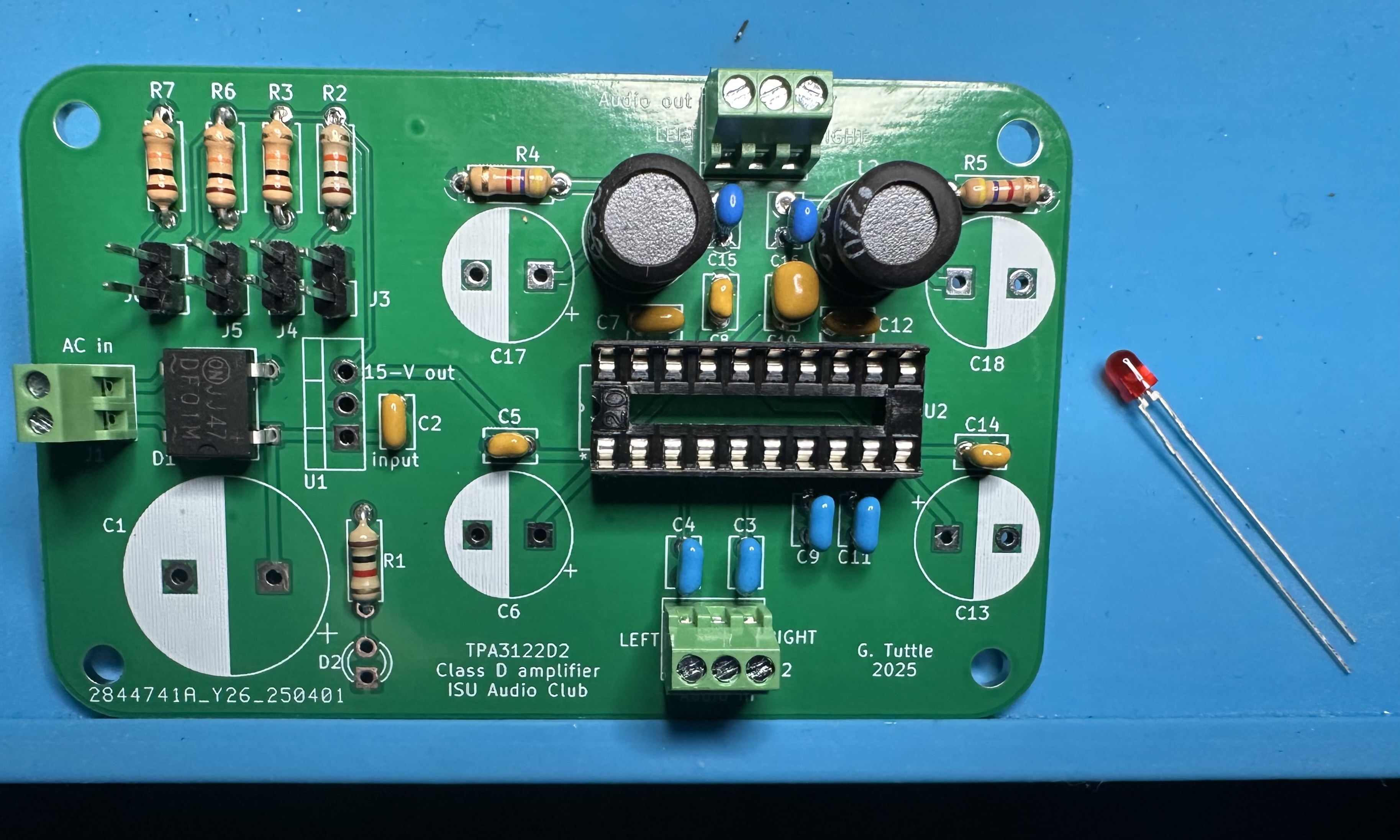
- Add the LED power indicator, labeled D2 on the board. (Recall that this is optional. Leave it out if you want.) Recall that the longer lead corresponds to the postive terminal of the diode. The longer lead should connect to the LED current-limiting resistor; the shorter lead connects to ground.
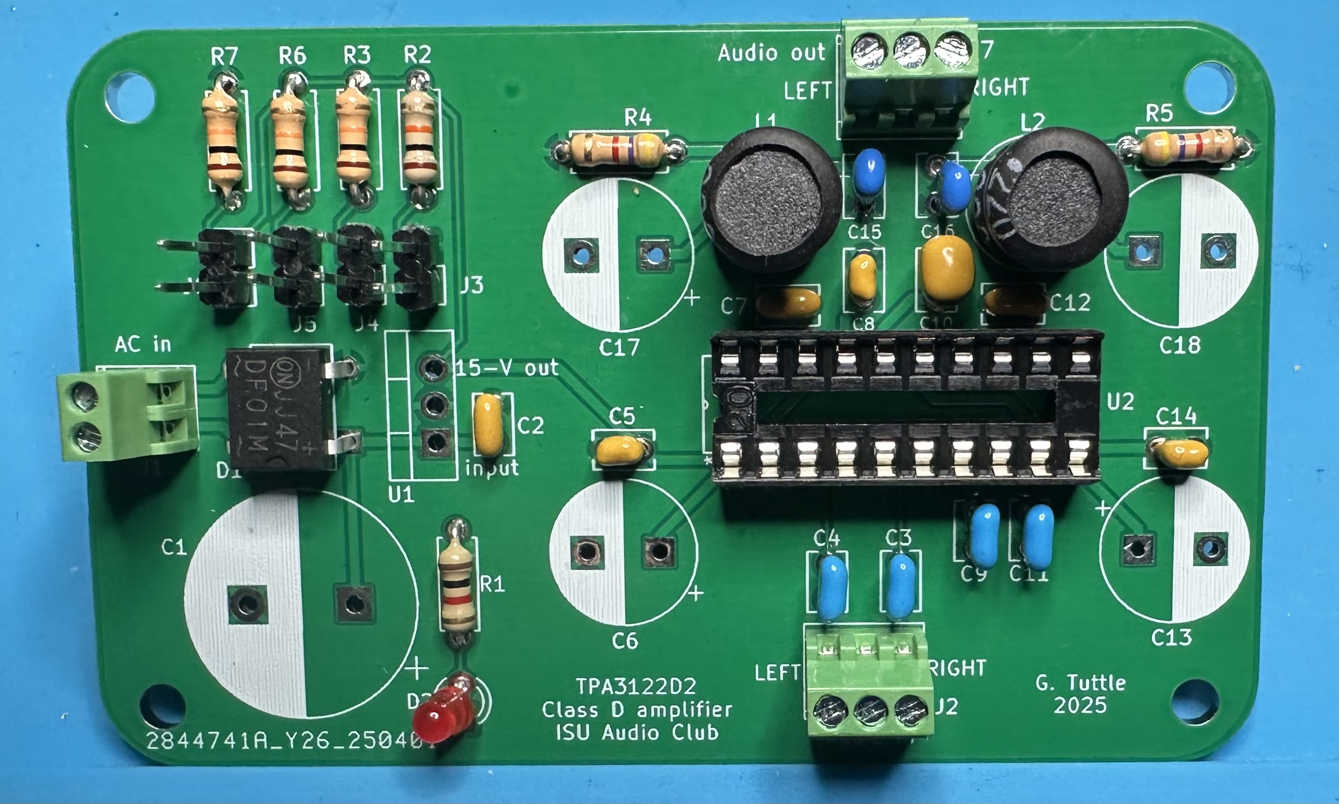
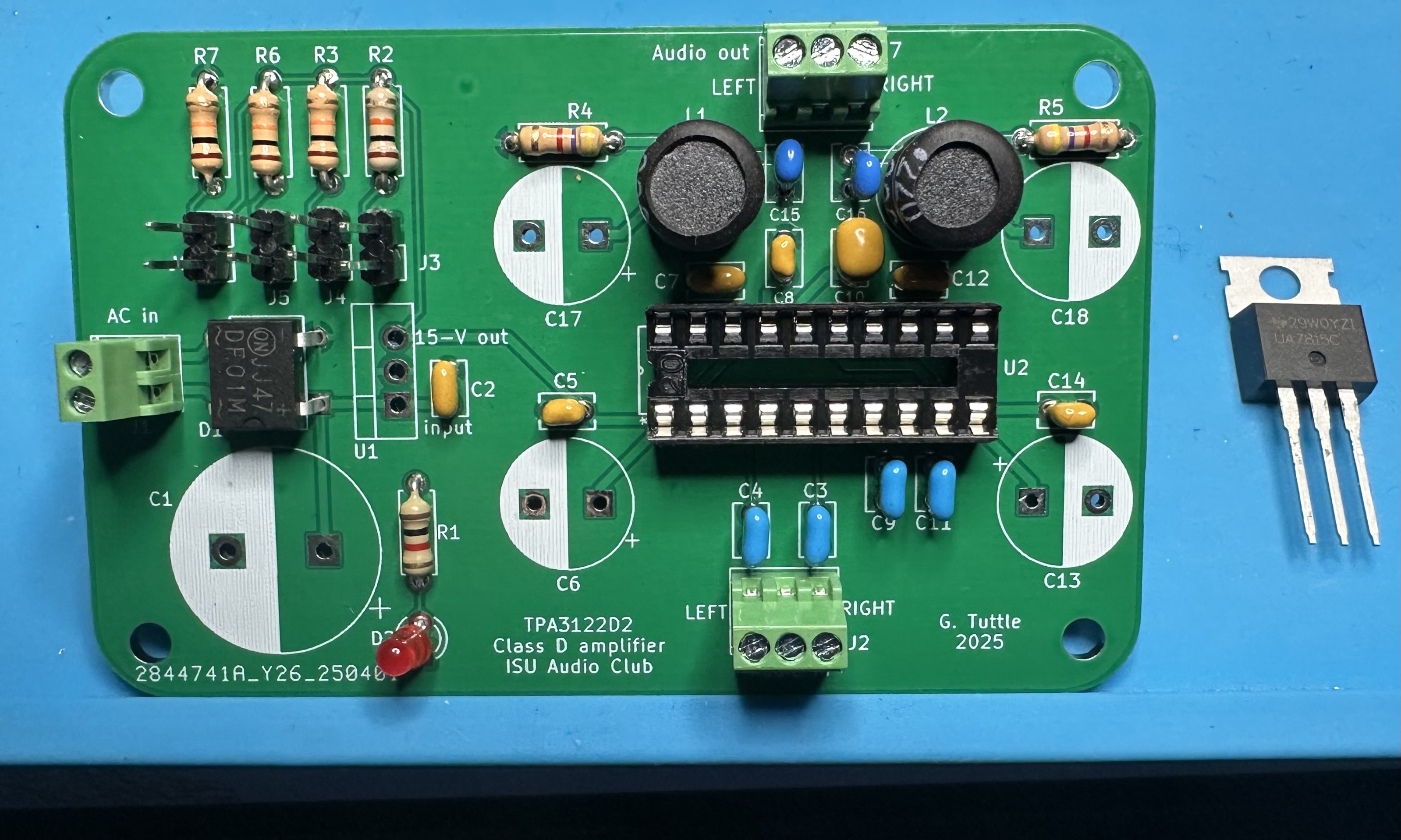
- Next, add the 15-V regulator part. It is labeled U1 on the PCB. Be sure to solder it in with the correct orientation. As you hold the part with the lettering facing you, from the left to right, the three pins are input, ground, and output. The lettered side should face capacitor C2.
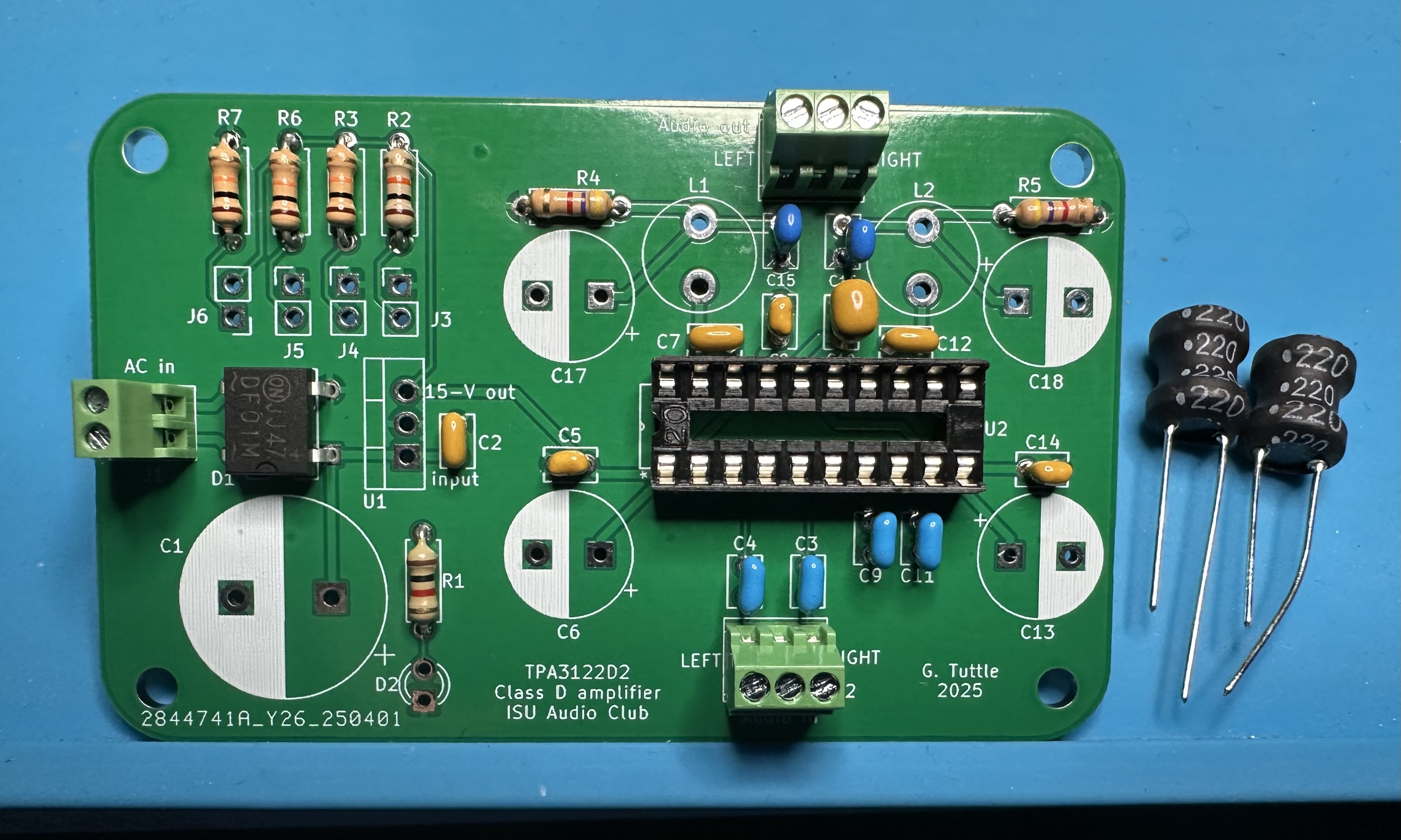
- Nearing the end! Four 470-μF capacitors are needed. C6 and C13 serve as bypass capacitors to smooth variations in the power voltage caused by power transistors switching on and off. C17 and C18 couple the output voltage to the speakers.
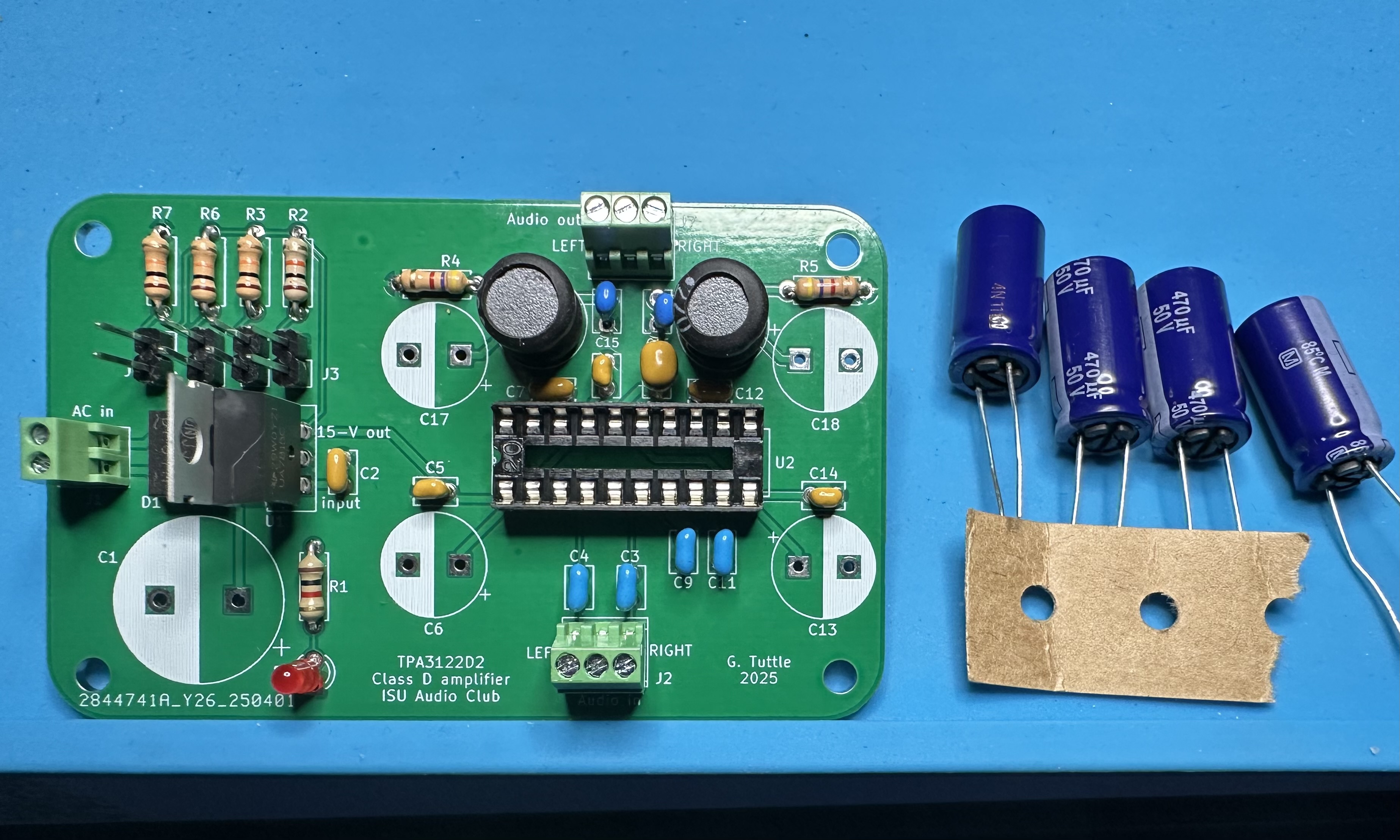
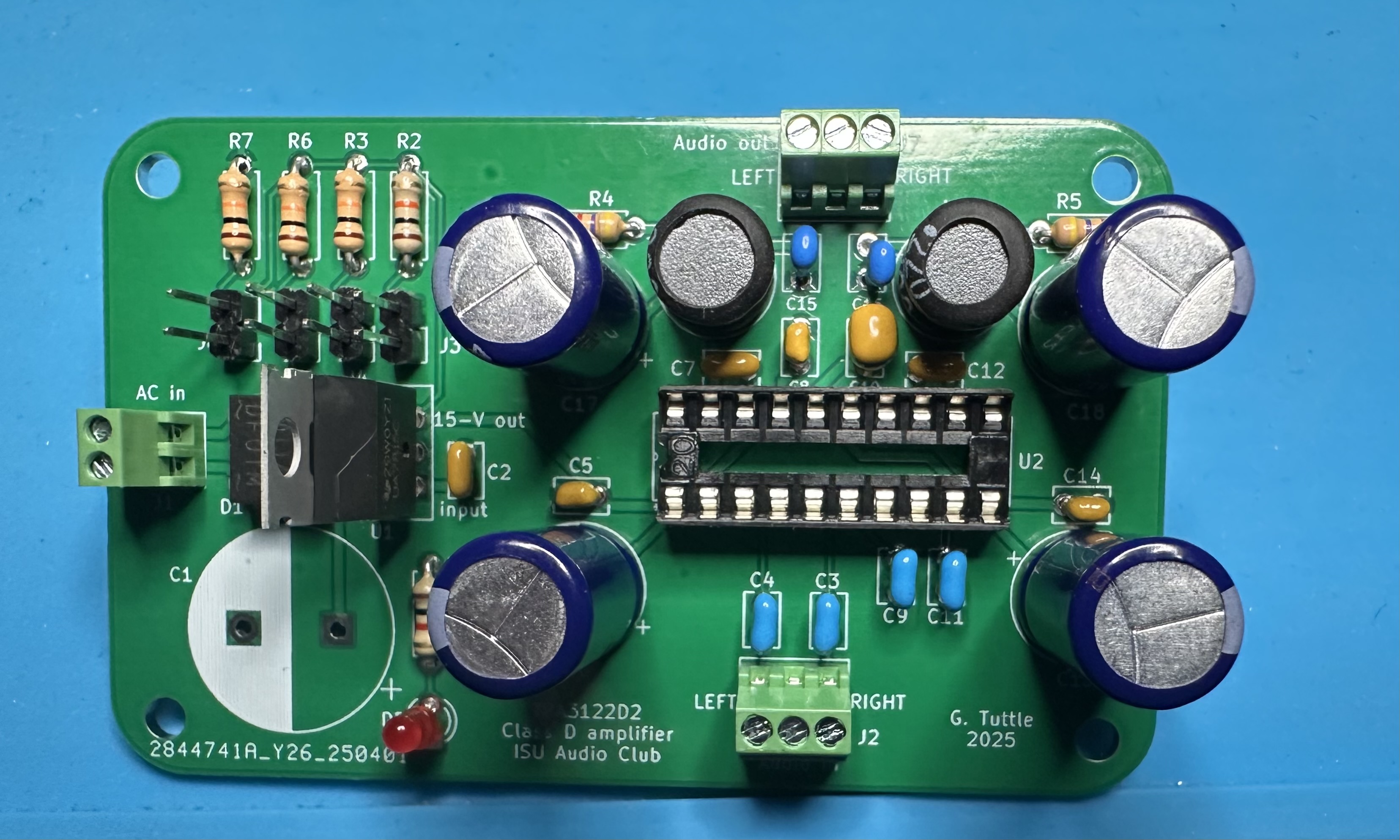
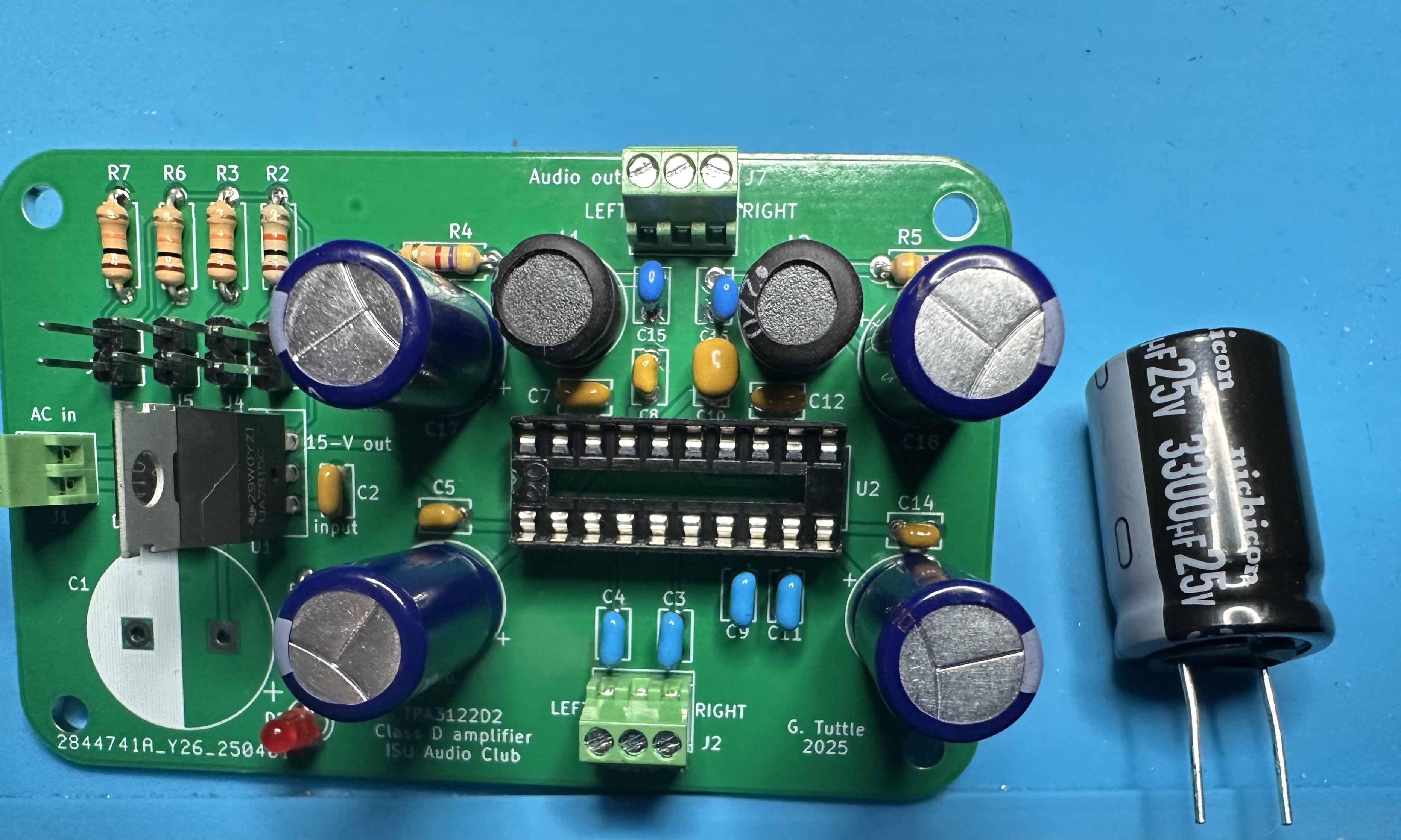
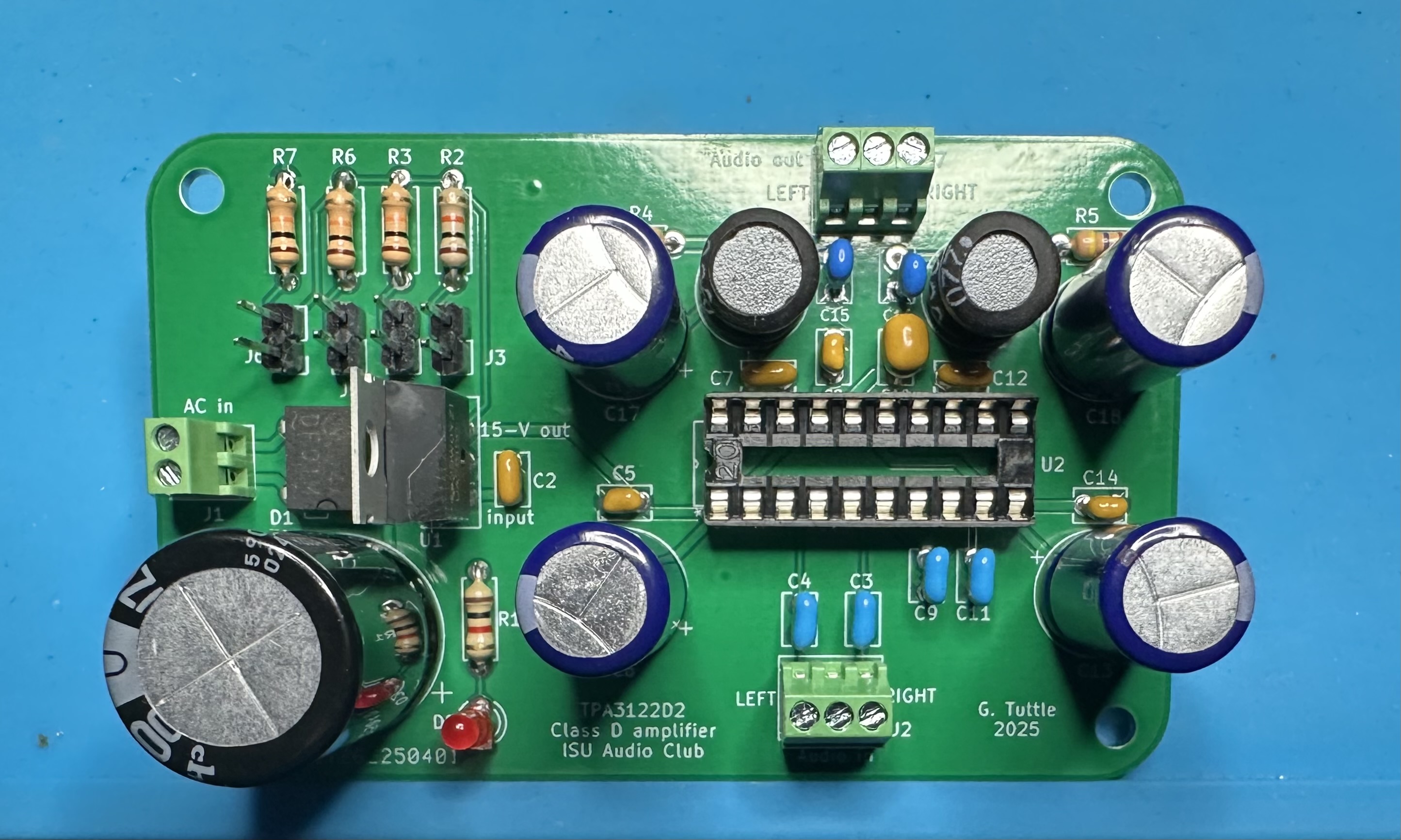
- Finally, we add the biggest component, a 3300-μF capacitor, labeled C1, that smooths the rectified AC power input.
- As a safety check, you might consider applying power to the board before inserting the class-D chip. Power can come from a 12-V RMS transformer or from an 18-V DC supply. When power is applied, the LED should light up. In checking DC voltages, you should find 15 V on pins 1, 10, 16, and 17 of the chip. Pins 7, 8, 11, and 20 should be at ground.
- When ready, insert the TPA3122 chip into the socket. (Or solder it in place, if you aren't using a socket.) Put the four jumpers on the header pins to short them together. With all four jumpers in place, the gain is set at 10 and the mute and showdown are not active. Apply power and begin audio testing you would like to do. Or hook up a source and speakers and see how it sounds!